Category: Driver Chip
Quad Stepper Motor Driver ◆Driver 4 motors at the same time. ◆Glitch filters on all inputs. ◆Low EMI emission.
+86-755-23067791
1. Overview
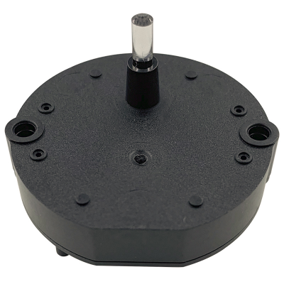
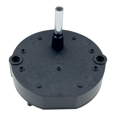
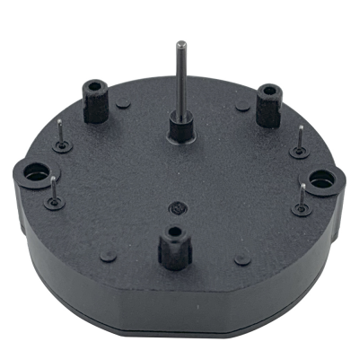
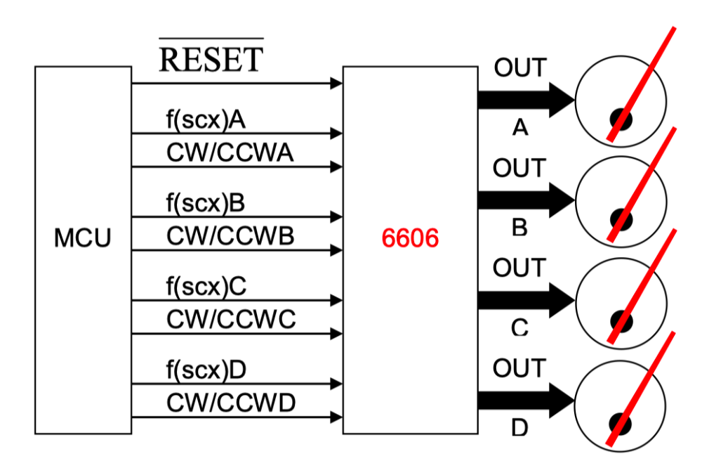
The quad stepper motor driver, 6606, is a monolithic CMOS device intended to be used as an interface circuit to ease the use of MDR29, MDR23 and MDR28 series stepper motor.
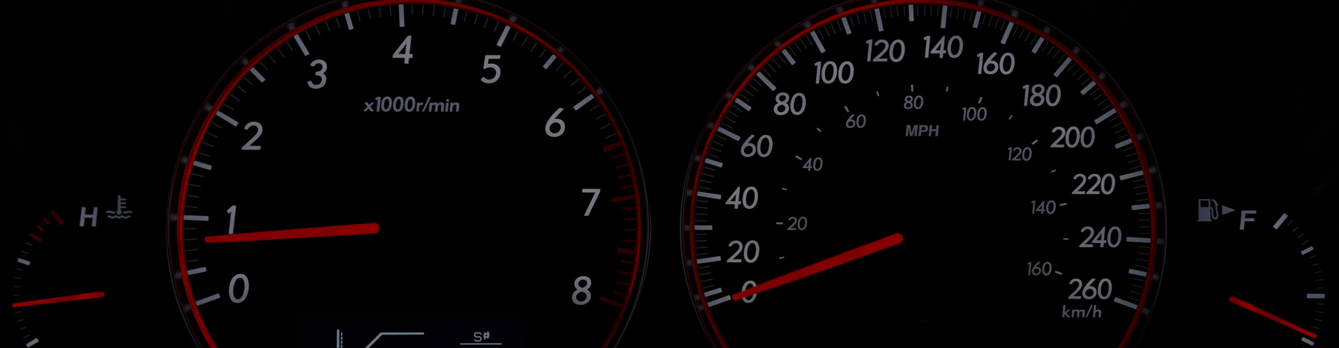
It is specifically designed for applications in automobile instrument cluster.
The chip allows the user to drive 4 motors at the same time as it contains 4 identical drivers on the same chip.
2. Operating Diagram
3. Pin Description
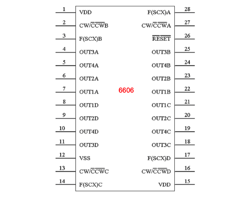
*Unused inputs must always be tied to a defined logic voltage level.
|
Pin Number
SOP - 28 |
Name |
I/O |
Function |
|
1/15 |
VDD |
V |
Positive supply voltage |
|
12 |
VSS |
V |
Negative supply voltage |
|
28/3/14/17 |
f(scx) A/B/C/D |
I |
Stepping frequency; Driver A / B / C / D |
|
27/2/13/16 |
CW/CCW A/B/C/D |
I |
Direction of rotation; Driver A / B / C / D |
|
26 |
RESET |
I |
Reset for the four drivers |
|
4/5/6/7 |
OUT 3A/4A/2A/1A |
O |
Output driver A |
|
8/9/10/11 |
OUT 1D/2D/4D/3D |
O |
Output driver D |
|
18/19/20/21 |
OUT 3C/4C/2C/1C |
O |
Output driver C |
|
22/23/24/25 |
OUT 1B/2B/4B/3B |
O |
Output driver B |
4. Circuit Protection
To filter fast voltage transients, it is highly recommended to connect two 100nF ceramic capacitors to the power supply pins, one on either side and as close as possible to the chip.
Moreover, to protect the chip against latch-up, a 5uF capacitor per motor connected should be added. Thus, for 4 motors, typically a 22uF capacitor must be used, either electrolytic or tantalum. Note this capacitor can be placed close to the voltage regulator.
Electrical Characteristics:
VDD = 4.5~5.5V, TA = -40~105°C, unless otherwise specified.
|
Parameter |
Symbol |
Test Conditions |
Min |
Typ |
Max |
Units |
|
Typical supply current |
IC |
VDD=5V,ω=200°/S, TA=25℃,RB25=280Ω |
|
76 |
|
mA |
|
Worst case supply current |
ICMAX |
VDD=5.5V,RESET=VSS, TA=-40℃,RB-40=190Ω |
|
|
200 |
mA |
|
Quiescent supply current |
ICC |
All inputs at VDD or VSS, no load |
|
|
300 |
μA |
|
Low level input voltage |
VIL |
VDD=4.5~5.5V |
VSS |
|
1.35 |
V |
|
High level input voltage |
VIH |
VDD=4.5~5.5V |
3.15 |
|
VDD |
V |
|
Input leakage |
IIN |
VIN=VSS or VDD |
-10 |
|
10 |
μA |

Copyright © 2020 MDR International Limited. All Rights Reserved. Designed by BATEN